
Fixing the GaN Problem
Another supply chain emergency on the horizon
In the semiconductor industry, the Trump administration is striving to bring back critical technologies that slipped out of our hands decades ago. The U.S. has attracted billions of dollars in investment to stimulate cutting-edge logic manufacturing, the development of EUV lithography, and HBM production. However, the semiconductor ecosystem is a lot more than just AI chips. And if the administration wants secure supply chains, it should focus on another rising material: gallium.
Just as Pluto is technically not a planet, gallium is technically not a rare-earth element despite often being discussed in the same context. Like many rare earths, gallium is not directly mined from the Earth’s crust but rather a byproduct of aluminum extraction. Although not classified as a rare earth, the mineral plays a major role in compound semiconductors and has critical importance for the future of AI, defense, robotics, and more.
China has realized the element’s importance and has quietly shored up its supply chain while the U.S. has been asleep at the wheel. Now, the U.S. must secure this critical mineral and its downstream technologies before another lead slips from our hands.
The Problem
China’s recognition of gallium as a priority — both for domestic development and weaponization against adversaries — is unmistakable. As a result of their efforts, China is responsible for 99% of raw gallium production today.
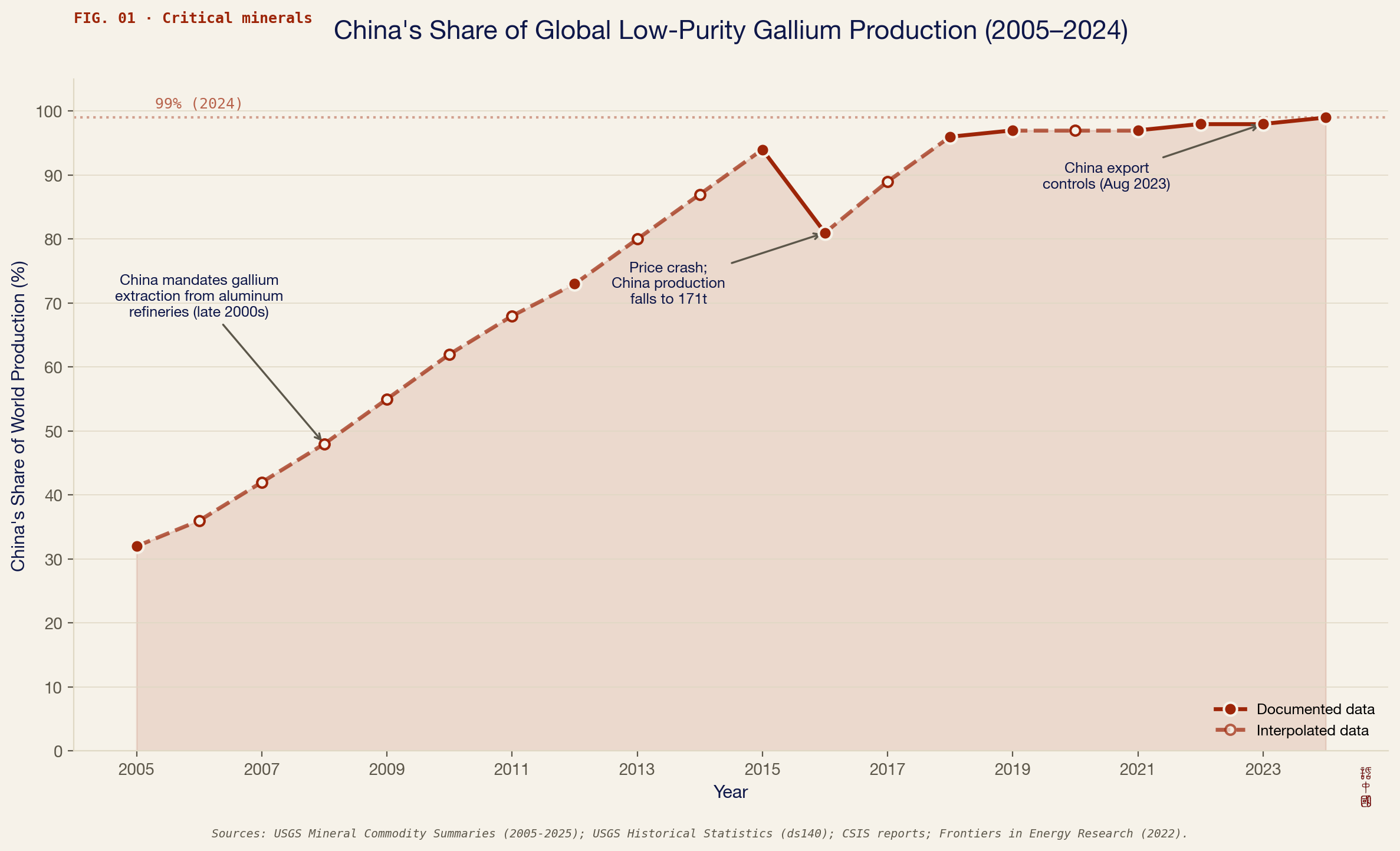
Since the early 2000s, China has required domestic aluminum producers to also extract gallium, which has enabled the country to not just become self-sufficient but dominate the global market for gallium extraction. In the meantime, the U.S. has not shored up its supply chain insecurities, particularly in upstream extraction, leaving America vulnerable to weaponization of the mineral.
Such vulnerability is not just hypothetical. China noticed its leverage and imposed export restrictions on gallium (and the tools to extract it) since 2023. These export controls wreaked havoc on gallium prices in the global market, and firms have reported trouble in securing licenses for required gallium. As China builds up dominance over the products downstream from gallium, the United States should be worried about a future where industries are cut off from critical semiconductors and begin working now to ensure that such a threat is neutralized.
This is the current story for upstream gallium — the mineral itself. America’s dependence on China for upstream gallium has been covered excellently by other institutions like CSIS and the Atlantic Council. To address this dependence, the U.S. must actually follow up on its many ongoing projects to produce gallium domestically.
However, a less-discussed security issue is looming: the dangers facing downstream gallium — that is, the products made from gallium. China’s downstream gallium semiconductor industry has begun to encroach on the viability of American and allied companies. Instead of panicking when it’s too late, the U.S. must address its impending downstream gallium crisis in tandem with its already-existing upstream gallium problem.
The Downstream Competition
Gallium in Power Semiconductors
What is gallium used for, and why has China emphasized it so much? The mineral forms the backbone of semiconductors like gallium nitride (GaN) and gallium arsenide (GaAs) chips, which are irreplaceable for certain defense, power, and optoelectronics applications.
One of the most critical of these uses — and the one most under threat — is in power semiconductors, typically using gallium nitride (GaN). GaN chips used for power functions are often referred to as GaN high electron mobility transistors (HEMTs). GaN HEMTs, though currently a limited market, are increasing in popularity due to their use in EVs, motor control for robotics, and power solutions for data centers. Currently, their biggest market is the consumer end-market, focused on products like fast chargers for your laptop and phone. While consumer end-markets will likely remain GaN’s biggest cash cow, it punches above its weight in terms of irreplaceability for humanoid robotics, data centers, and EVs.
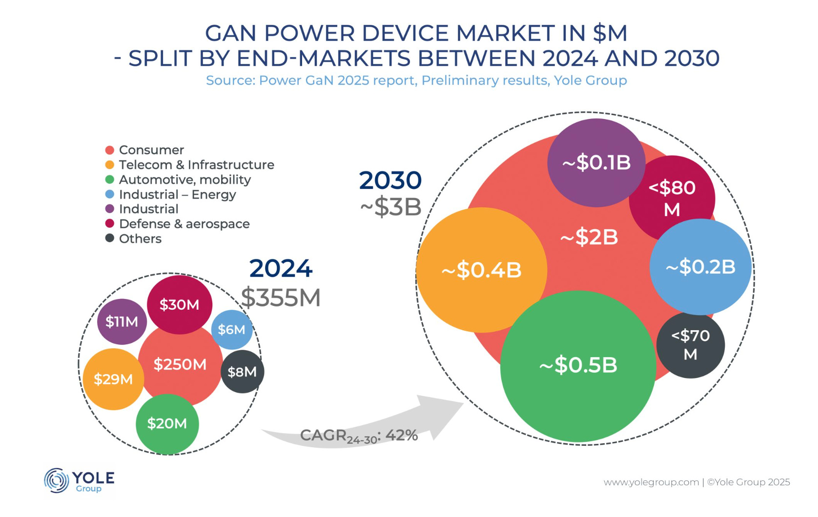
GaN, alongside silicon carbide (SiC), is considered a wide bandgap semiconductor, which endows it with properties better for power electronics compared to standard silicon. These properties include faster switching and better power efficiency. Although SiC chips are able to stand in for GaN in some contexts, GaN for power is largely irreplaceable due to its faster switching and better performance at lower voltages. Generally, SiC is used in heavy-duty applications like large industrial robotics, whereas GaN is used for lower-voltage applications like smaller humanoid robots.
Innoscience’s Rise
With respect to GaN power semiconductors, the U.S. has already lost its lead and is at risk of being pushed out altogether. Like the story with solar panels and electric vehicles, the U.S. (alongside Europe) built up a lead in the “higher-value” segment of products by being a first-mover, but the lead was promptly chipped away as sprouting Chinese companies buried American firms with unbeatable prices.
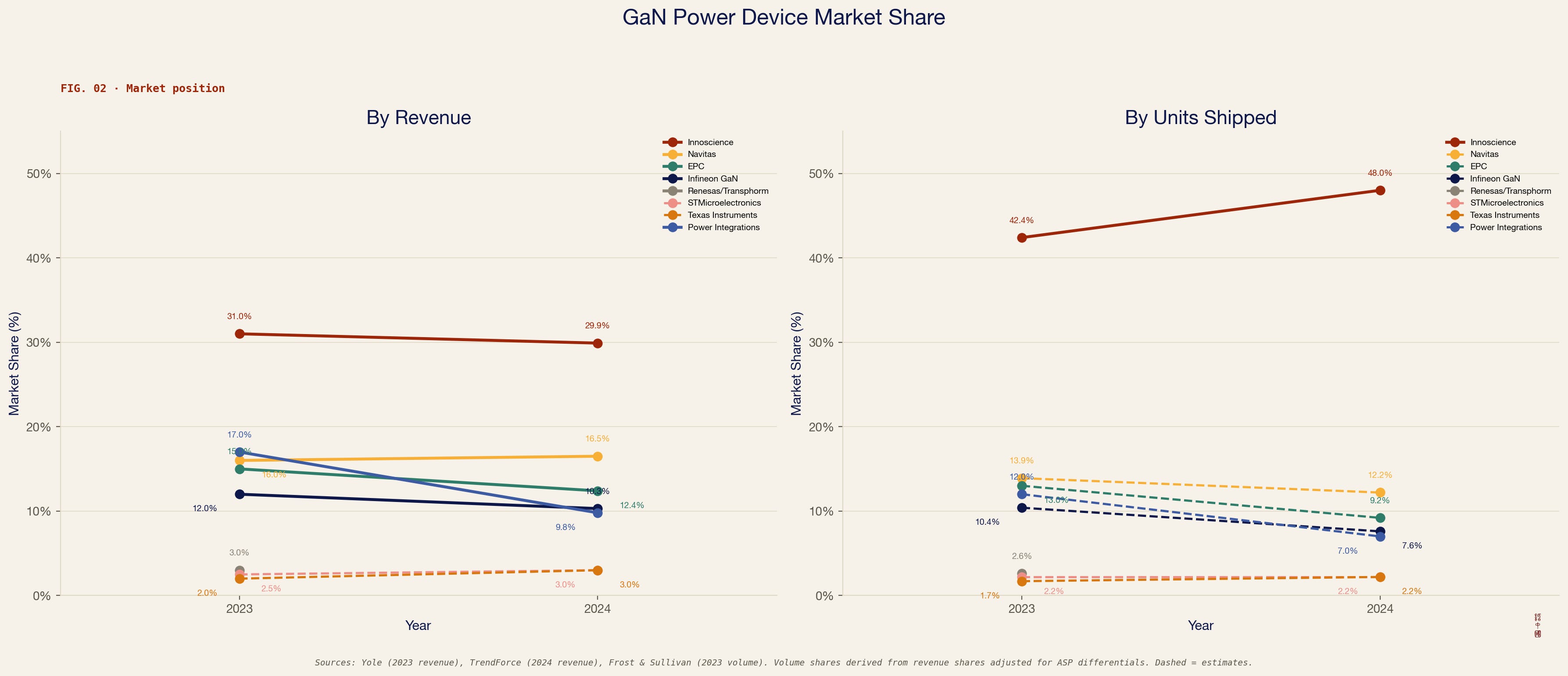
Here, the main competitor is Innoscience (英诺赛科), a Suzhou-based GaN integrated device manufacturer (IDM), whose prices are nearly 50% lower than competitors’. As a result, Innoscience now leads the global market for power GaN chips, beating out the American Navitas and EPC and German Infineon. Other players like STMicroelectronics and Onsemi have bent the knee to Innoscience by giving up packaging expertise, system integration, and their own manufacturing capacity in exchange for access to Innoscience’s production facilities in China.
As Innoscience continues to expand capacity, the situation risks shifting from one of market dominance to one of market monopolization. If trends continue, competition in the GaN power market will become a fiction, constituting a national security threat to the U.S.
So, how is Innoscience so much better than its competitors? The answer boils down to the synergy of in-house manufacturing, a stomach for unprofitability, government support, and genuine innovation.
In the GaN market, AMD co-founder Jerry Sanders’s adage holds true: real men have fabs. After Innoscience, the other two leading GaN makers include the American companies Navitas and EPC. Both are fabless. Both must rely on external foundries for their chips, which increases the cost of their final products.1
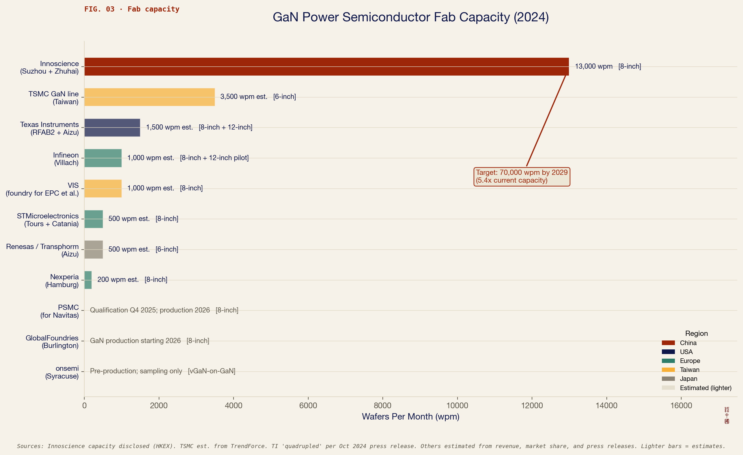
From the beginning, Innoscience decided to spend the money on R&D to make its own fabs, and its bet has paid off. Both Navitas and EPC have relied on TSMC for its fabrication, but TSMC is now exiting the GaN market entirely. Now, their business is getting punted off to Taiwan’s Powerchip (PSMC) and American GlobalFoundries because TSMC realized its capacity was better used for the more lucrative AI chip market.
Fab capacity for GaN is trending toward Innoscience holding all the keys. By being the first to mass-produce 200mm GaN wafers, the unit economics are in Innoscience’s favor. Compared to the previous standard of 150mm wafers, 200mm wafers allow for up to 80% more chip output at 60 to 70% of the cost. Further, by being first to the scene, Innoscience has had more time to perfect its process, achieving a yield of about 97% whereas others are stuck below 90%. Innoscience’s capacity also blows competitors out of the water, producing nearly four times as many wafers as second-place TSMC. With Innoscience having no intentions to slow down, the unit economics will just get better and better for the Chinese IDM and worse and worse for everyone else.
Companies like Onsemi and STMicroelectronics realize that the cheapest way to fabricate their designs is through Innoscience, creating a dynamic that essentially positions Innoscience as the TSMC of GaN. The question now is how much longer can Navitas and EPC find fabs that aren’t Innoscience to fabricate for them? And then in the long term, why would Innoscience ever want to fabricate for a direct competitor when it could instead monopolize the GaN power market? Even for Onsemi and STMicroelectronics, after market consolidation, Innoscience may devour its children.
Innoscience was able to become the greatest GaN company by being willing to stomach unprofitability. In 2021, the company was operating with a gross margin of over negative 266%. Unlike Western companies, Innoscience — and its funders — have been willing to eat bitterness while it figured out its manufacturing process, increasing yield and expanding capacity. American markets do not have the same willingness. Other GaN makers have been incentivized to maximize profit margins in the short run while Innoscience chased viability over the long run, leading to where we are now.
Now, Innoscience has been able to capitalize on its high-yield manufacturing process and exploding demand for GaN for high-tech applications to achieve positive margins for the first time in its history. Although the company likely won’t turn a profit until 2027, the upward revenue trend contrasts Innoscience with that of other GaN players. (Quarterly revenue from GaN sales alone is not available for some companies.) And if Innoscience was not deterred by negative margins in its early years, the company will most definitely not be deterred now.
Part of Innoscience’s perseverance in the face of negative margins is due to assistance from government subsidies. The combination of investments from national and provincial state-backed funds has totalled over 350 million dollars of financial support at minimum for the then-burgeoning Innoscience. That is more than double the company’s gross losses since 2021. By the time of its IPO in 2024, the company had established enough capacity and was already poised as the best option for large-scale GaN manufacturing. Other companies like STMicroelectronics realized this, and they decided to become a cornerstone investor in Innoscience with a $50 million investment and further fund the GaN giant.
But before we lazily blame the evaporation of Western market share on government subsidies, we must reckon with the reality that Innoscience has also simply played better than the U.S. Competition in the GaN power market is more intense for individual voltage ranges. Some companies, like EPC, focus only on the sub-350V range. (Products in the sub-100V range are used for motors in humanoid robots, sensors and ADAS for electric vehicles, and motherboard power conversions in data centers.) Most companies expand that focus up to 650V or 700V. However, Innoscience is the only company that both designs and manufactures GaN power chips across the whole spectrum, from 15V up to 1200V.
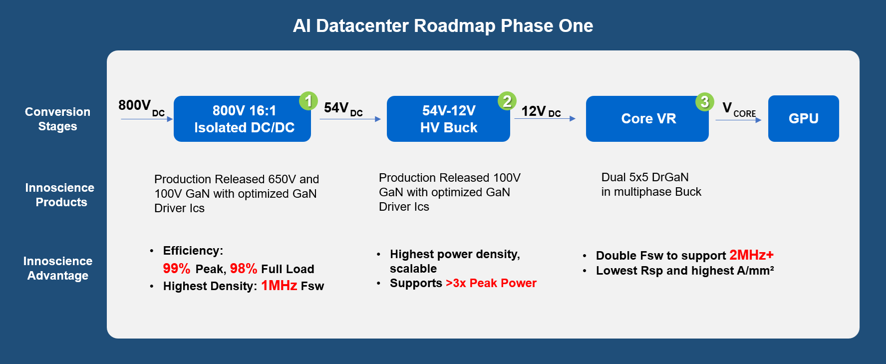
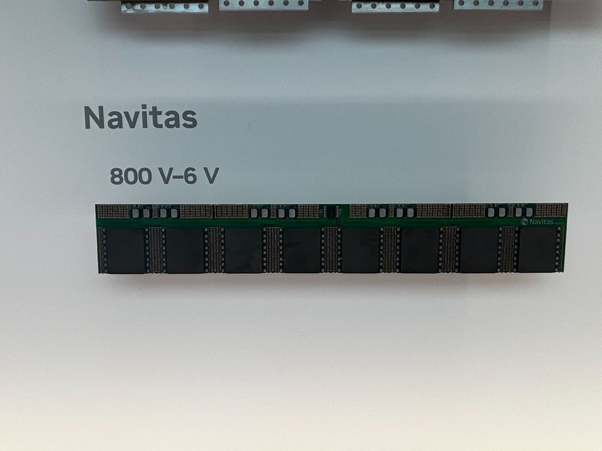
And they are not low-quality chips, either. For example, Innoscience designs and produces 650V and 100V GaN products for rack-level power conversion in AI data centers. Innovation in this increasingly critical segment enabled Innoscience to become Nvidia’s sole Chinese partner for this power architecture. The 800 VDC power architecture is touted as the best option for the “next generation of AI factories” because it allows better power efficiency and less reliance on copper cables. Although large companies like Nvidia will always qualify more than one supplier for diversification, Innoscience will likely emerge as a primary supplier if its prices and quality remain preeminent.
Lest I risk fearmongering, it is important to note that none of these 800 VDC GaN designs by any company have been qualified as of this piece’s publication. They are all simply reference designs that Nvidia has requested from these companies. A rudimentary analysis also suggests that Innoscience’s competitors have created better products for this application; for example, Navitas’s product supports an output of down to 6 V, suggesting better capabilities for handling high current. It is unclear how important this functionality is and what the cost differential is for these products. If any reader with a background in GaN would like to provide answers, please comment or reach out to aqib@chinatalk.media.
Regardless, such innovation cannot be swept aside and blamed on government subsidies; the U.S. must contend with Innoscience as a company with the ability to both produce at scale and innovate. These characteristics enabled Innoscience to establish its partnership with Nvidia (and now Google) for the future of AI data centers.
And regardless of the extent of government subsidies enabling Innoscience’s rise, the U.S. cannot just call foul play and say it isn’t fair. There is no referee. We must take fate into our own hands and fix the problem ourselves. The U.S. has prided itself on government programs such as DARPA shepherding critical technologies like GPS and the Internet before they were profitable. Can we not do the same for manufacturing critical technologies like GaN?
We now find ourselves in a position where the snowball is forming. If we do not prevent it from getting bigger, makers of robots, EVs, and data centers may reasonably be dependent on a single Chinese company for its power chips. Do we seriously believe these technologies will become less important in the future? In the next trade war or diplomatic spat, this is worrying leverage that China could use to bottleneck critical industries. Does this not mean we should be trying to stimulate GaN production, not throw its carcass to the vultures?
The Solution
Fortunately, it is easier to fix the problem now, when we still have some GaN players, compared to later, when the outcome is set in stone. To ensure the U.S. is not overreliant on China for critical GaN products, we must support allied industry to make producing GaN a profitable venture. We should perhaps limit competition in the short term to create healthy competition and stable supply chains in the long term. This does not mean the extermination of Innoscience, but rather the protection of market competition.
Policy should also recognize its limitations, however. The U.S. cannot and should not spend obscene amounts of money to compete with China on capacity. Instead, we must focus on winning on efficiency, innovation, and other methods that give us the edge besides raw buildouts.
Patent Infringement Cases
The quickest relief is through the judiciary. Both EPC and Infineon have filed patent infringement cases against Innoscience, and the results of those cases could limit Innoscience’s ability to compete in the American market. Although EPC’s claims were invalidated by the USPTO, import restrictions imposed by the ITC continue to be enforced. The Infineon case will be finally decided on May 7 by the ITC as well.
The ITC’s determinations, however, will not be a panacea. The patent infringement punishments only apply to certain products, and Innoscience would be able to design around them to continue to sell in the U.S. Further, the determinations would not be able to restrict finished products containing Innoscience chips. Especially when the current money makers — consumer end-products — are largely produced in China, the case determinations may not produce a serious impact. This route is also not a policy position, as the judiciary should not bend the rule of law for policy goals.
The Race to 300mm
Outside of the judiciary, the U.S. can support innovation and the commercialization of the next generation of GaN power semiconductors. Here, the best options for champions are Texas Instruments and Infineon. Both companies have dedicated foundry space for GaN power semiconductors, and both have piloted the production of 300mm GaN wafers. Where Innoscience was able to achieve superiority in unit economics from the shift from 150mm to 200mm wafers, TI and Infineon can perhaps achieve it in the shift from 200mm to 300mm.
However, the gains from 200mm to 300mm may not be as large as the gains from 150mm to 200mm. Although 300mm wafers produce about 2.25 times as many chips per wafer compared to 200mm, the throughput for processing may not be as high. For epitaxy, 300mm wafers currently require single-batch processing due to strict requirements for wafer uniformity and robustness, whereas 200mm wafers allow for multi-batch processing. Development of multi-batch 300mm wafer tools is almost certainly ongoing, but no progress is yet visible. The overall cost savings and throughput advantages of the 300mm transition are still unknown, but they may not be as impressive as the previous 200mm transition. The step to 300mm is a step toward the ultimate objective for GaN manufacturing — cost-parity with silicon — and it is an important step toward reducing dependence on Innoscience. However, it is not a panacea.
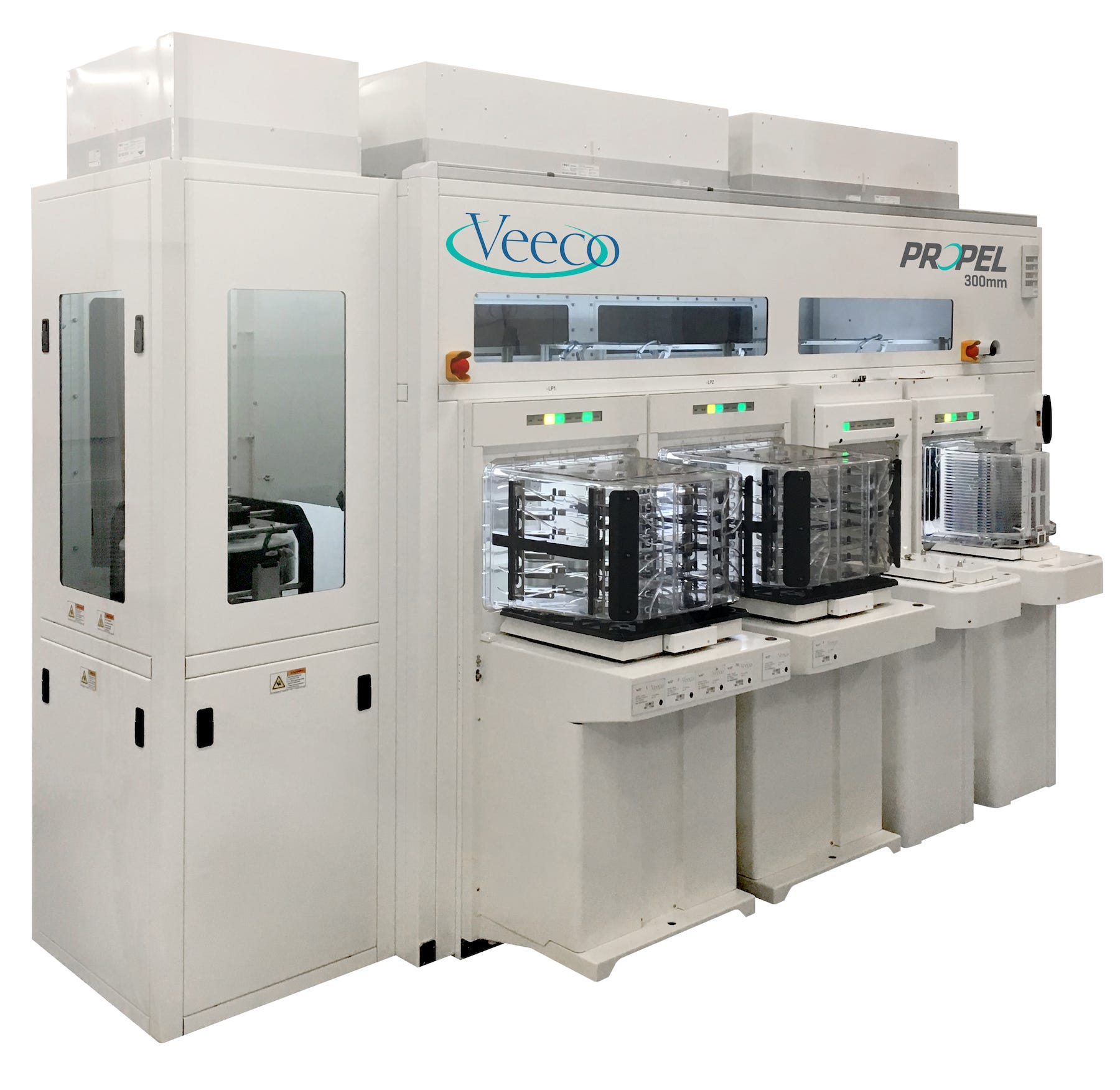
America’s export controls on the metal-organic chemical vapor deposition (MOCVD) tools required for GaN epitaxy (ECCN 3B001 a.2.) may enable the 300mm wafer lead to be enduring. Infineon and TI have been able to achieve pilot production because they have been able to purchase the relevant MOCVD equipment from the German AIXTRON and American Veeco, whereas Innoscience must wait for domestic suppliers like AMEC to develop a solution. AMEC has no visible progress toward 300mm GaN, so export controls will perhaps give TI and Infineon more time to develop and mature process flows for 300mm GaN.
To goad TI and Infineon on, the U.S. may fund projects through the CHIPS Act to support the quicker construction (or conversion) and operation of 300mm GaN fabs. By accelerating the timeline to mass production, homegrown companies will more quickly improve yields and unit economics so Innoscience’s explosive capacity expansion would not be so oppressive. We cannot build as much as Innoscience, but perhaps we can build better.
Ecosystem Stickiness
The most enduring solution would be to create ecosystem “stickiness” for end-customers so that they are more locked into purchasing from allied companies. The West again has an inherent advantage here, with allied GaN makers (mainly U.S.-based Texas Instruments and Germany’s Infineon) being IDMs across the semiconductor stack; unlike Innoscience, they do not solely focus on GaN.
For end uses more complicated than fast chargers (e.g., data centers and robotics), GaN becomes less of a commodity and more a question of integrated solutions and technical capabilities. End customers would be more willing to work with GaN suppliers that could tailor their manufacturing solutions to the customers’ power architecture, which presents an opportunity to reduce the importance of Innoscience’s price lead.
For example, when a company wants to purchase a GaN power HEMT for their humanoid robot, they should be incentivized to purchase a system, not just the product. If they are already using a TI MCU, it should pair best with TI’s gate driver ICs, TI’s sensor chips, and TI’s GaN HEMTs. By contrast, there is no such thing as an Innoscience MCU. When the full-stack comes with so many advantages, customers are incentivized and better served by sticking with TI, rather than considering redesigns to drop in a cheaper Innoscience product.
Innoscience simply does not have this ecosystem capital outside the GaN stack, and unless they quickly partner with Chinese companies across the stack, they will not accumulate such capital soon. Currently, they must rely on products from companies like TI and Taiwan’s YAGEO for reference designs of motor drives.
To capitalize on this ecosystem advantage, the U.S. could consider providing modest funding for better open reference designs for applications like robotic motors, EV onboard chargers, and data center power topologies. Companies are already incentivized to pursue this, and TI already does this well, but coordinated government funding could reduce barriers and promote better designs. If the U.S. produces powerful reference designs that perform well with potential robotics MCUs, data center power topologies, POL parameters, and vehicle architectures, then end-customers may not care about the marginal savings of Innoscience’s GaN HEMTs.
The primary source of pessimism with this strategy, however, is that American reference designs may not matter if the end-customers are Chinese. If Unitree and BYD are the main end-customers, they will likely work with Chinese MCUs (like ARTERY) and be incentivized to work within the Chinese ecosystem. The American GaN market will miss out. This is not a fait accompli, however. Chinese carmakers like Changan Automobile have opted for American Navitas GaN chips for their onboard chargers, meaning Chinese OEMs can be incentivized to pick American products over Chinese ones.
Further, larger companies like hyperscalers tend to have their own engineers who do not need to rely on the easy reference designs given to them; they make bespoke designs in house and take the best products for each segment, prioritizing cost savings and performance over ease of use.
Still, funding design is significantly cheaper than funding factories, and better reference designs may trickle down to benefits for start-ups in the robotics industry where the major players have yet to calcify.
Flexible Fabs
Lastly, though most vaguely, the U.S. should incentivize companies to make it as easy as possible to convert legacy fabs into GaN fabs if the need arises, just as we did with factories during World War 2. Although this would mostly be easy, as GaN wafers can be processed by the same equipment used in depreciated legacy fabs, the biggest obstacle would be ramping up the epitaxy for GaN wafers. In this case, possible options include encouraging a GaN wafer stockpile or promoting expedited production of MOCVD equipment for GaN epitaxy.
Conclusion
The U.S. is largely aware of its upstream gallium dependency, and 99% dependence is a difficult ditch to climb out from. But let’s ensure that we do not fall into the same ditch when it comes to GaN.
The U.S. can accomplish long-term viability in the GaN market now before Innoscience makes it too difficult. We can accomplish this through innovation and flexibility, not expensive buildouts, via the pursuit of 300mm wafer adoption, ecosystem stickiness, and flexible fabs. These are not the only tools in the toolbox, but they are feasible options that the U.S. government could readily pursue.
We also do not need — and probably should not want — to banish Innoscience. American and allied companies like Onsemi and STMicroelectronics work with Innoscience, and punishing one would be punishing the whole lot. Instead, we should focus on preventing Innoscience from becoming a monopoly and encourage companies to work within the American ecosystem instead of compelling them to settle for a Chinese one. A world with Innoscience and at least one allied viable alternative is a win.
Instead of sleeping at the wheel (again), the U.S. can prevent GaN from going the way of solar panels and EVs. If we want to secure our supply chains, we can start with GaN.
The author would like to thank several GaN industry executives for their contributions to this piece.
For those wondering why the fabless business model does not bring efficiency games, the reason is the real efficiency gains come from fabless firms relying on a pure-play foundry. In this case, the foundry can maximize unit economics and pass on savings to fabless firms. In GaN, this is not the case because of the small size of the GaN market. Fabs like TSMC are not incentivized to make GaN in large quantities or on large wafers, meaning the savings passed on are minimal. Innoscience’s model reflects the philosophy of being the size of a large pure-play foundry that will be serviceable in the future though a money-loser now.
Nice piece. After reading it I want to print it off and stick it in my copy of "Chip War" by Chris Miller.
The ST and Onsemi deals strike me as more dangerous than the Nvidia headline. Once Western chipmakers start routing their own production through Innoscience's factories, any future policy move has to push back on two sides at once: China, and the US-allied companies that have already decided cheapest-at-Innoscience is the right commercial call. Very hard to unwind once the capex is committed.