
How Far Can Chinese HBM Go?
Given export controls, what HBM node can China reach?
This December, we’re teaming up with GiveDirectly to send cash to 800 impoverished families in the Bikara region of Rwanda. Studies show that direct cash transfers have a multiplier effect of 2.5x in local economies and reduce infant mortality rates by 48%. Your donation is also tax-deductible in the United States. The link to give is here, and the deadline for donations is midnight on December 31st. Please consider donating if you can!
Aqib Zakaria is a researcher focused on semiconductors, AI, China, and Taiwan. He holds a Master’s degree in Regional Studies — East Asia from Harvard and was recently a summer fellow at the Centre for the Governance of AI (GovAI).
High-bandwidth memory, or HBM, remains the key bottleneck for China to catch up in manufacturing advanced AI chips. As Moore’s Law has more or less held steady, logic nodes have continuously progressed.
However, the rate of memory chip progression has been slow compared to logic chips. Thus, AI operations are often “memory constrained,” meaning that compute is sitting idle waiting for the memory chip to feed it data on which to perform operations. HBM was created to address this “memory wall” by stacking multiple memory chips on top of each other to boost memory bandwidth. As AI chips continue to get better, HBM remains a critical component for scaling. Simply put, if you care about the AI race and AI chips, then you must care about HBM.
Although China’s memory champion CXMT has been closing the HBM gap, the three memory giants of SK Hynix, Samsung, and Micron continue to be more than two generations ahead of CXMT’s HBM2. Assuming export controls hold steady, China’s HBM advances will continue to be stymied by a lack of advanced equipment.
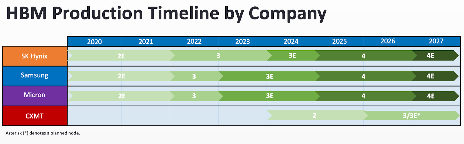
For perspective, achieving the industry’s current HBM3E and HBM4 would be a tremendous achievement for China. As of November 2025, the most advanced AI chips in use use HBM3E. H100s, B100s, and other leading GPUs tap into HBM3E for memory, while Nvidia’s upcoming Rubin GPUs will use HBM4. If CXMT can achieve HBM4 quickly, then they will be able to crack a key part of making advanced GPUs. However, even if they are able to make HBM4 several years down the line, competitive AI chips will likely have meteored beyond contemporary standards to handle workloads unimaginable today.
Ray Wang’s piece earlier this year in ChinaTalk mapping CXMT alongside other memory giants helps policymakers keep an eye on China in the rearview mirror. But past HBM2, when will CXMT hit a wall? Given the current state of export controls and Chinese technological development, what node of HBM can China be expected to reach?
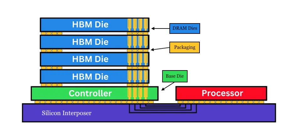
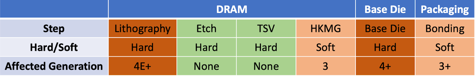
The Three Ingredients: DRAM, Base Die, and Packaging
Making HBM is a difficult endeavor, and the product’s performance ultimately comes down to three factors: the DRAM dies that compose the HBM, the base die that routes the signals coming in and out of the memory stack, and the packaging that binds the DRAM dies together.
Different bottlenecks exist within each of these three HBM components that will hinder CXMT’s progress at different HBM generations. Each merits its own discussion.
DRAM
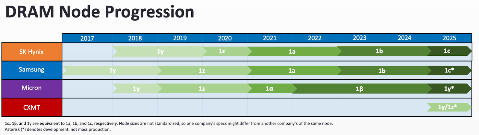
The memory industry uses a different terminology to mark node sizes compared to the logic industry. Instead of referring to a node by nanometer, the DRAM industry has begun to use letters for its advanced nodes. They started first with 1x, then 1y, and then 1z; afterward, they moved to the Greek alphabet, with 1α after 1z, and then 1β, and then 1γ. (Samsung and SK Hynix use the English 1a, 1b, and 1c instead, but this article uses Micron’s terminology.) Just to demonstrate the gap between each generation, between Micron’s 1β and 1γ nodes, the product speeds increased by 15% while reducing power usage by 20%.
As of 2025, CXMT is three generations behind the leading memory manufacturers, making the 1z node while the big three are shipping 1γ. With the 1z node, however, CXMT can produce DRAM for HBM up until HBM3.
But what must CXMT do to achieve beyond the 1z node? To get to 1α and beyond, CXMT must shrink DRAM cells even further, which requires advanced tools in lithography, etching, and deposition.
Lithography
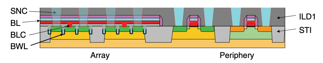
Two of the most difficult steps in DRAM manufacturing are forming the bitline contact (BLC) and storage node contact (SNC). The BLC is the physical connection between periphery transistors that decide what memory needs to be fetched to amplify their signals and the capacitors that actually hold the memory.
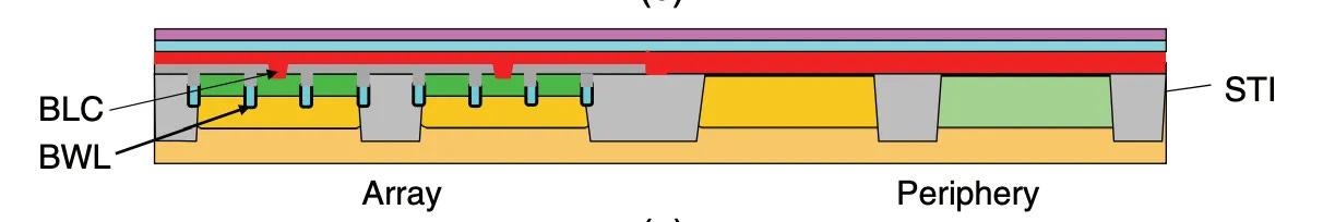
As shown above, patterning and etching the BLC must thread the needle so as to contact the source/drain of the array transistors rather than the buried wordline (BWL) shown in teal.
The case is similar for the SNC, the physical connection between the bitline and capacitor. As shown below, the SNC must be etched through layers of different materials to again connect with the source/drain of the array transistors, instead of the BWL.
As DRAM nodes progress, the pattern density and critical dimensions of these processes get stricter, and greater precision is required. Eventually, EUV lithography is needed for these processes.
However, Micron has used techniques like self-aligned quadruple patterning (SAQP) to continue to use DUV up until its 1β node. Chinese manufacturer SMIC has used similar techniques to stretch DUV use for advanced nodes in the past, like its 7 nm Huawei chip. CXMT is likely even better at utilizing SAQP given the memory industry’s lengthier history with the process. Even for 1γ, Micron only uses EUV for one layer of the process, likely either the BLC or SNC step.
Thus, CXMT can likely also stretch its DUV use until 1β. After that, considering Micron has attempted to delay EUV use until the last possible moment, 1γ and beyond will become extremely difficult without access to the export-controlled EUV equipment. Without EUV, advanced nodes will either be impossible to make or of terrible yield; according to some estimates, using EUV, while more expensive, saves about 3-5% yield for advanced nodes while decreasing process steps by 20-30%. Without EUV, CXMT’s progress in DRAM will likely be stalled at the 1γ node, meaning HBM4E and beyond will be difficult for China to achieve from the DRAM standpoint alone.
Etching
For etching, the picture looks more favorable for CXMT. Advanced etching is required for the steps above, as well as for creating capacitor holes. These holes, which hold the memory charges, have small critical dimensions, high pattern density, and are very deep. Etching narrow yet deep holes like this can lead to a variety of defects, shown below, and thus require advanced tools with high aspect ratios (ratio of height to diameter). Aspect ratios reached 40:1 in the 1x era, with estimates for advanced nodes closer to 60:1.

The U.S. has imposed export controls on advanced etching equipment, including anisotropic etchers (the ones needed for capacitor etch), though China has been able to domestically produce equipment defying the controlled parameters.
For etching through silicon nitride for the capacitors, BLC, and SNC, Chinese products include Naura’s Accura NZ and Accura LX, as well as AMEC’s Primo nanova. Technical specifications about Chinese products are not widely available, though the Primo nanova is specifically advertised for the 1x node and beyond. Although this means the product probably cannot be stretched to cutting-edge nodes, Naura’s tools may work well enough.
Regardless, the existing Chinese offerings demonstrate that China is not too far behind on equipment for capacitor etch. These tools are susceptible to having exaggerated capabilities or scaling issues with manufacturing, but, especially compared to lithography, they’re not so far behind. China holds 10% of the global dry etch market and is self-reliant for about 15% of its advanced etching needs. The country’s rapid growth in the industry also demonstrates that etching obstacles may not be so solid. In short, China’s HBM progress will probably not be meaningfully hindered by DRAM etching bottlenecks.
Beyond etching, advanced deposition tools are required for DRAM manufacturing, but the story is very similar to etching: China can already produce the tools required, so it will likely not be a bottleneck. China is self-sufficient for 5-10% of its deposition needs and is also rapidly accelerating its indigenization efforts.
Through-Silicon Vias (TSVs)
Another step in DRAM manufacturing for HBM is the formation of through-silicon vias (TSVs), diagrammed below. This front-end-of-the-line process forms the vertical connections that allow stacked DRAM dies to communicate and function together. Without TSVs, the concept of HBM and of nearly all advanced packaging would be impossible.
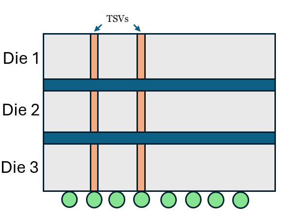
For making TSVs, the most important process again is etching. TSVs require precise etching through DRAM dies to later deposit the material that serves as the vias connecting all the wafers together. The U.S. has imposed export controls on etching equipment specifically for TSV formation (EC 3B001.c.4), but again, China’s domestic manufacturers have been able to defy these parameters.
TSV critical dimensions currently range from 3-5 µm with depths of less than 100 µm. As nodes progress, DRAM dies are getting thinner, and both the depth and CD will decrease. Currently, China already offers equipment to satisfy these TSV requirements. AMEC’s TSV300E advertises a TSV CD of down to 1 µm and can achieve depths of several hundred microns. Naura’s PSE V300, though not publishing its specs, likely achieves a similar performance. Chinese product specs may be exaggerated or with lower throughput, but empirically, TSVs do not seem to pose an issue for CXMT given its capacity rivals other leading memory makers.
Having already achieved likely self-sufficient capabilities in TSV formation, CXMT will not be bottlenecked from this step in HBM manufacturing.
High-κ Metal Gate (HKMG)
Another process difficult in DRAM manufacturing is implementing the high-κ metal gate (HKMG). As shrinking DRAM cells for performance gains becomes increasingly difficult, HKMG has served as another means to increase device speeds.
As shown below, periphery transistors on a DRAM die are normally advanced by shrinking distances between the source and drain while also thinning the gate insulator. However, when insulator thinness reaches its limit, leakage issues emerge, and HKMG is used to solve them.
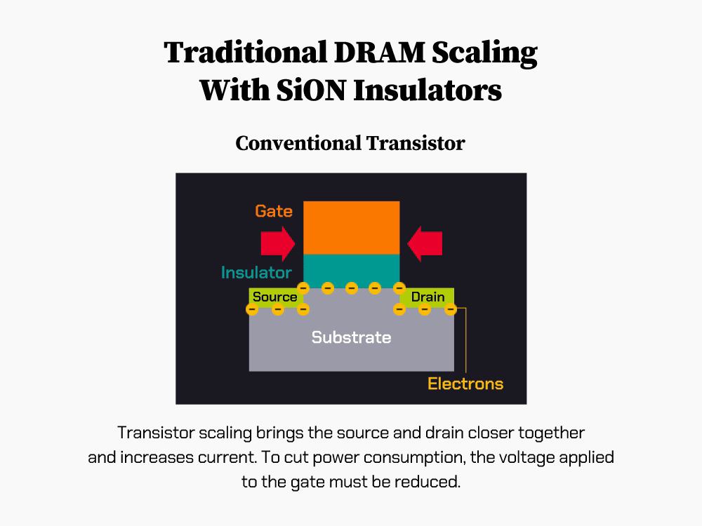
HKMG replaces traditional gate materials in periphery transistors to accelerate electron flow and prevent power leakage. Partially due to implementing HKMG, SK Hynix was able to achieve a 33% boost in speed with a 21% decrease in power usage.

The HKMG process has been adopted by memory makers since, and CXMT is now beginning its adoption process too; however, some reporting indicates that CXMT is struggling with its HKMG implementation, leading to reduced yield and slower manufacturing ramp-up. Other memory makers have adopted HKMG in their process flows around the 1z node, where CXMT is stuck now, so the company must hurdle the HKMG barrier to keep pace.
Incorporating HKMG in DRAM processes is difficult, partially because of the simultaneous processing of the periphery and array on a single wafer. The thermal budget of the array, or how much heat the structures are able to withstand, is relatively low; this means that the standard HKMG processes for logic nodes cannot be so replicable for DRAM. Although CXMT is currently struggling with HKMG, this doesn’t seem like an insurmountable issue. The bottleneck seems to be the more amorphous challenges of experimenting and perfecting process flows rather than a concrete wall of equipment inaccessibility. The equipment required for HKMG generally relates to the deposition tools in which China seems more or less self-sufficient.
Because of the lack of “hard” barriers like lack of access to tools, HKMG adoption will likely not be a serious hindrance to China’s HBM advances.
Base Die
The HBM DRAM dies sit on top of the base die. Among other functions, the base die routes signals coming in and out (I/O) of the memory stack. Ultimately, regardless of how strong the memory dies are, the power of the base die determines the upper limit of memory bandwidth for HBM.
As HBM nodes have progressed, the number of pins on the base die has increased, along with the data transfer speed of those pins. As a result, memory makers have used more advanced DRAM nodes to function for the base die to satisfy the requirement. Around the HBM4 generation, though, memory makers are compelled to use more expensive logic nodes to handle the workload. As such, memory makers are now partnering with TSMC to manufacture their base nodes for advanced generations.
The advanced logic nodes used for base dies will pose a problem for CXMT in its HBM advancement. Without EUV lithography, SMIC has been struggling to advance beyond 7 nm without abysmal yield.
For HBM4, CXMT can retrace Micron’s steps and continue to use a 1β DRAM die for base die functions. However, this decision would have significant drawbacks. Not all HBM4 are created equal, and by using a memory-process base die, Micron has emerged with HBM4 worse than SK Hynix and Samsung. While Micron’s product meets the JEDEC minimum of 8 Gbps per pin and goes to 9 Gbps, SK Hynix and Samsung have been able to reach 10 Gbps per pin and beyond via logic node base dies. Micron claims that they have begun sampling HBM4 with 11 Gbps, but Irrational Analysis explains why this is probably misleading.
Regardless, Micron has conceded that memory nodes are not best suited for the base die after HBM4 and has partnered with TSMC to produce the base die for HBM4E on an advanced logic node. For CXMT, this likely means that using 1β DRAM dies for HBM4 will result in a subpar product, and that HBM4E will be difficult to make without SMIC making breakthroughs in logic nodes.
However, lower cost HBM4 and 4E may be possible for CXMT. Although memory makers are producing their most advanced base dies for HBM4 at 5 nm and below, they are also offering alternatives with cheaper 12 nm base dies. 12 nm base dies can get the job done, but the products with more advanced logic offer smaller interconnect pitches for memory performance and lower power consumption. These make the 5 nm base dies attractive for AI workloads desired by customers like Nvidia.
Although CXMT could theoretically partner with TSMC for its base dies, as they would likely not fall under export control restrictions, my conversations with experts suggest that TSMC may not accept such orders given geopolitical tensions. Essentially, without access to advanced logic nodes for the base die, CXMT will likely struggle to make competitive HBM4 and HBM4E. They will likely be able to make HBM4 with non-leading-edge 12 nm base dies. Perhaps they will even be able to secure orders from TSMC for advanced nodes, but the amount of question marks here makes CXMT’s success uncertain.
Packaging
Packaging is how the entire HBM stack comes together, and one element in particular is relevant. The “glue” that binds DRAM dies to each other, or bonding, is critically important. Stacking so many dies together creates thermal issues that bonding plays an important role in addressing; further, more efficient bonding with minimal gaps between dies is important to enable further stacking. As HBM has evolved from stacking only four dies to now up to sixteen, efficient bonding has been a key enabler.
Die Bonding
A possible struggle for CXMT will be succeeding in die bonding, but not because of export controls. Currently, export controls do not restrict the sale of bonding equipment used for HBM.
The two primary methods for die bonding in HBM are thermocompression bonding with non-conductive film (TC-NCF), used by Samsung and Micron, and mass reflow-molded underfill (MR-MUF), used by SK Hynix. SK Hynix adopted MR-MUF early on since HBM2E, and because of the decision, SK Hynix has been consistently lauded as creating superior HBM.
MR-MUF involves heating and connecting all the stacked dies at once, rather than one at a time like in TC-NCF. The real magic potion for MR-MUF, though, is the epoxy molding compound (EMC) used to fill the gap between dies.
MR-MUF has both better throughput and thermal dissipation than TCB. This is important both to scale production of HBM, but also to manage its heat requirements. By using MR-MUF, SK Hynix is able to stack more dies with fewer usage problems. HBM failures are the number one cause of AI chip failures, so MR-MUF to manage heat grants a real competitive edge.
Following SK Hynix’s footsteps, CXMT is reportedly adopting MR-MUF for its HBM3 and beyond; however, adoption is not like flicking a switch. To reap the benefits of MR-MUF, CXMT must solve several issues. First, MR-MUF is inferior to TC-NCF in managing die warpage. As DRAM dies become even thinner, CXMT will take time resolving this issue, just as SK Hynix has. SK Hynix solved this issue with a process it calls “advanced MR-MUF,” which adds a step of temporary bonding to the process — a step which CXMT may imitate.
Secondly, material acquisition may pose a problem. Competition, not export controls, may bar CXMT from acquiring the EMC for MR-MUF. SK Hynix has an exclusive deal with the Japanese materials company NAMICS for providing its EMC. SK Hynix’s material has been co-developed over years with NAMICS, and the material must be suited for each company’s process flow. Some Chinese sources suggest that CXMT’s EMC supplier is the domestic company Huahai Chengke (华海诚科), but this is still unconfirmed. Even if CXMT uses a domestic supplier, it will likely take years to work together to achieve a high yield.
Because of the extra steps from DRAM making to die bonding via MR-MUF, CXMT’s yield for its HBM3 in 2026 will likely take time to ramp up. Some experts claim that CXMT’s HBM3 yield likely won’t break 40% until the latter half of 2026, partially because of the MR-MUF adoption process.
In the end, though, CXMT’s early bet on MR-MUF will likely turn out to be a good idea in the long term, if not the short term. The advantages of the process are clear, and the bonding process only seems to be a short-term stumbling block. Though not a strict bottleneck, adopting MR-MUF will likely cause CXMT to slow production of HBM3 and beyond, but will not serve as a bottleneck for advanced generations.
Unanswered Questions
It is difficult to gauge CXMT’s capabilities or breakthroughs with 100% certainty. Unlike Chinese model developers, China’s chip manufacturers like to play their cards close to their chest. Because of the sensitive nature of their work, which is relevant for national security goals, or perhaps just because of the nature of the industry, CXMT rarely makes public statements. Perhaps this will change if CXMT undergoes its IPO as planned in 2026.
As such, certain details about China’s memory ecosystem are unanswerable without insider information. Some specific questions are listed below, and ChinaTalk invites anyone with color to reach out with answers or leads:
DRAM Node Sizes
What are the critical dimensions of the latest DRAM nodes and their aspect ratios?
What are the critical dimensions for TSVs in the latest HBM generations? How many TSVs are now included on a single DRAM die?
Chinese Equipment Ecosystem
How good are AMEC and Naura’s etching equipment for mass production? How good is China’s deposition equipment in practice? How true are the advertised specs?
CXMT Struggles
What part of HKMG adoption is CXMT struggling with?
Who is CXMT’s EMC provider for MR-MUF?
If anyone has answers to any of these questions, or has information related to prior analysis, please respond to this email or reach out to jordan@chinatalk.media!
Conclusion
Overall, CXMT is progressing at a steady pace for making HBM, but this trend is likely not to hold forever. For each step of the HBM process — DRAM, base die, and packaging — different bottlenecks will appear to stall CXMT’s progress or compel them to make sub-par HBM. First, the lack of advanced logic for base dies will likely lead CXMT to make lagging-edge HBM4. Even if CXMT utilized a memory node for its base die for HBM4, this would result in an estimated 10% decrease in memory bandwidth. After HBM4, both the base die constraint and the lack of EUV for DRAM manufacturing will cause trouble.
Summary of Conclusions:
But CXMT should not be written off. The industry chose HBM as the best option for memory in AI chips because it was the path of least resistance. With export controls, that may not be true for CXMT and China. Other alternatives for alleviating the memory bottleneck have been discussed, including using hybrid bonding, high-bandwidth flash (HBF), a unified cache manager (UCM), compute in memory (CIM), ferroelectric RAM (FeRAM), and magnetic RAM (MRAM). All of these options have their own problems and are nowhere near adoption, but they present opportunities for China to move off the beaten path and achieve memory self-sufficiency in its own way. If any U.S. administration reverses export controls, though, China will be able to more quickly follow the path for HBM development and catch up in the AI chip race.
For now, though, with HBM remaining the preeminent option, CXMT will have its work cut out for itself.
 | A guest post by
|
The HKMG barrier you mentioned is interesting because it's more about process mastery than hard equipment limits. That probably means CXMT could catch up faster there than with the EUV stuff, but it's still gonna slow them down in the near term. It's kinda like how they've worked around DUV limits before but this time the workaround needs way more refinement to get yields up.
Great note. We have a lot of tourists in semiconductor investing today and when the cycle turns a lot of folks are going to get hurt. If anyone reading this has capital at work in semiconductor and really wants to learn how the industry works, this is a superb place to start learning. Kudos. Alex.